Products & Technologies

Products & Services
Company
Contact
Back to Menu
Products & Services
Products & Technologies
Services
Resources
Company
Contact
MAKE POSSIBLE
Our blog is dedicated to a global discussion about the ideas, actions and technologies changing the world as we know it.
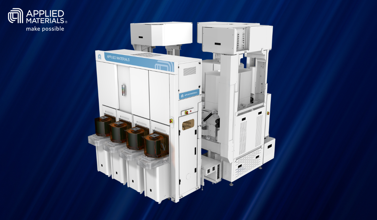
Building on an Unmatched Foundation of CVD Innovation
by Ajay Bhatnagar | April 11, 2024
In 1987, Applied Materials shipped the first Precision 5000 CVD (chemical vapor deposition) system – a breakthrough machine that revolutionized the deposition of the thin films at the heart of the chipmaking process. The internet was still a government research project and AI was the stuff of science fiction, but Applied’s innovative system laid the groundwork for many of today’s most advanced electronics applications.
Stay updated on our content.